

Product Details
Place of Origin: CHINA
Brand Name: ZMSH
Certification: rohs
Model Number: Germanium Substrates
Payment & Shipping Terms
Delivery Time: 2-4 weeks
Payment Terms: T/T
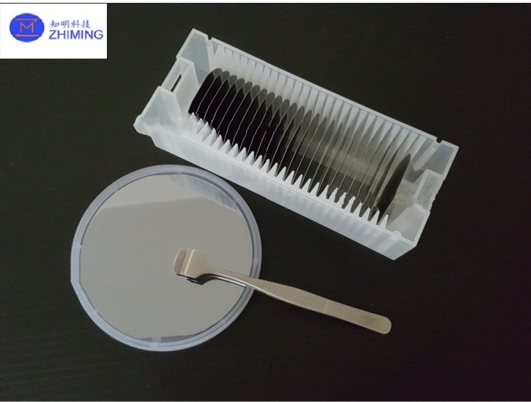
Materials:: |
Ge Single Crystal |
Diameter:: |
0.5~150mm |
Thickness:: |
0.5mm |
Type:: |
N-type/ P-Type/ Un-doped |
Surface:: |
Polished/etced |
Resistivity:: |
0.1~60ohm.cm |
Industry:: |
Semiconductor Substrates,device,optical |
Materials:: |
Ge Single Crystal |
Diameter:: |
0.5~150mm |
Thickness:: |
0.5mm |
Type:: |
N-type/ P-Type/ Un-doped |
Surface:: |
Polished/etced |
Resistivity:: |
0.1~60ohm.cm |
Industry:: |
Semiconductor Substrates,device,optical |
![]()
![]()
![]()

