

Product Details
Place of Origin: China
Brand Name: zmsh
Model Number: Gold Plated Silicon Wafers
Payment & Shipping Terms
Delivery Time: 2-4 weeks
Payment Terms: T/T
Material: |
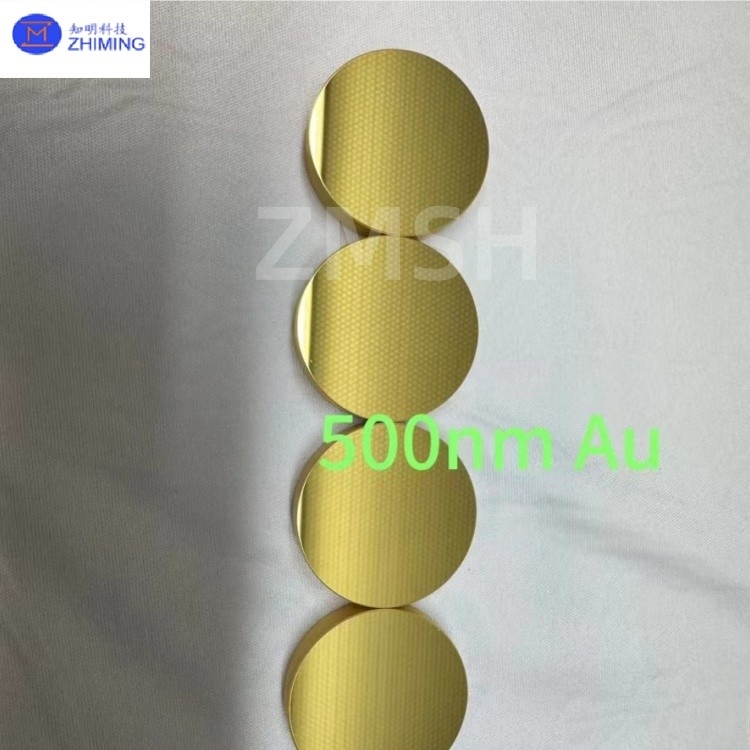
Au,Silicon Wafers |
Size: |
Customized |
Thickness: |
Customrized |
Crystalline Phase: |
110/111/100 |
Process: |
Magnetron Sputtering/thermal Evaporation/electroplating, Etc.; |
Structure:: |
Substrate + Adhesive Layer + Plating; |
Application: |
Grow Nanomaterials,Scanning Electron Microscope (SEM) |
Material: |
Au,Silicon Wafers |
Size: |
Customized |
Thickness: |
Customrized |
Crystalline Phase: |
110/111/100 |
Process: |
Magnetron Sputtering/thermal Evaporation/electroplating, Etc.; |
Structure:: |
Substrate + Adhesive Layer + Plating; |
Application: |
Grow Nanomaterials,Scanning Electron Microscope (SEM) |
| Size: | 2, 4, 6, 8 inches, others can be customized; |
| Process: | magnetron sputtering/thermal evaporation/electroplating, etc.; |
| Structure: | substrate + adhesive layer + plating; |
| Substrate material: | silicon wafer, quartz, BF33 glass, etc |
| Types of metal films: | gold Au, platinum Pt, aluminum Al, copper Cu, nickel Ni, silver Ag and other metal films; |
| Metal film thickness: | 10nm-10um; Common thickness: 100nm, 300nm, 500nm; Uniformity is better than 1%. |

