

Product Details
Place of Origin: China
Brand Name: ZMSH
Model Number: customized
Payment & Shipping Terms
Minimum Order Quantity: 10pcs
Price: by case
Delivery Time: 10-30 days
Payment Terms: L/C, T/T, Western Union
Material: |
Silicon |
Size: |
Customized |
Usage: |
Micronelectronic |
Application: |
Semiconductor Industry |
Shape: |
Customized |
Origin: |
Shanghai, China |
Material: |
Silicon |
Size: |
Customized |
Usage: |
Micronelectronic |
Application: |
Semiconductor Industry |
Shape: |
Customized |
Origin: |
Shanghai, China |
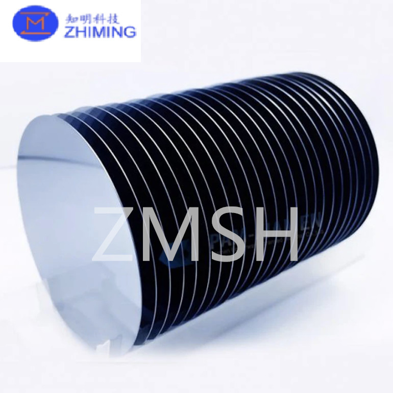
Silicon Wafer Silicon-On-Insulator Silicon Semiconductor Micronelectronic Industry Multiple Dimension
Product Description
In semiconductor manufacturing, silicon on insulator (SOI) technology is fabrication of silicon semiconductor devices in a layered silicon–insulator–silicon substrate, to reduce parasitic capacitance within the device, thereby improving performance. SOI-based devices differ from conventional silicon-built devices in that the silicon junction is above an electrical insulator, typically silicon dioxide or sapphire. The choice of insulator depends largely on intended application, with sapphire being used for high-performance radio frequency (RF) and radiation-sensitive applications, and silicon dioxide for diminished short-channel effects in other microelectronics devices.
![]()
![]()
Features
-Superior electrical performance: The SOI structure reduces the parasitic capacitance between transistors, reduces power consumption, and improves the switching speed, which is suitable for high-performance integrated circuits.
-Low power consumption: The ability of SOI technology to operate at lower voltages significantly reduces static and dynamic power consumption, making it suitable for mobile devices and other applications that require high energy efficiency.
-Good thermal management: The insulation layer of the SOI wafer provides better thermal isolation and improves heat dissipation performance, helping to improve the stability and reliability of the device.
-High integration: SOI technology enables a higher level of integration, making the design more compact and able to achieve more functions in a smaller area.
-Radiation resistance: SOI materials are less sensitive to radiation and are suitable for applications in aerospace and other high radiation environments.
-Good isolation: The insulation layer effectively reduces the interference between devices and improves the overall performance of the circuit.
![]()
![]()
Growth Method
1. SIMOX
SIMOX technology mainly consists of two processes. First, oxygen ions are injected into the silicon crystal to form a high-concentration oxygen injection layer. In order to prevent the silicon from crystallizing during the injection process, a certain temperature must be maintained in the substrate during the injection process. After that, high temperature annealing reduces or eliminates the defects generated by the injection, so that the injected oxygen reacts with the silicon to form an insulating layer, and then forms SOI. However, this process is expensive and has been gradually phased out.
![]()
2. BESOI
BESOI mainly consists of two process steps: (1) bonding: two polished silicon wafers with high-quality thermal oxide growing on the surface are strictly cleaned, and then bonded by using van der Waals force in a super-clean environment, and annealing at high temperature to improve their bonding strength; (2) Back thinning: with one piece as the substrate, the other silicon wafer is ground and polished to the required thickness to form a silicon single crystal film on the insulator.
The bonding mechanism of the process is that when two flat, hydrophilic surfaces (such as oxidized silicon wafers) are placed opposite each other, bonding occurs naturally, even at room temperature. It is generally believed that bonding is caused by the mutual attraction of hydroxyl groups (OH-) adsorbed on two surfaces to form hydrogen bonds. In order to increase the bond strength, subsequent heat treatment is also required, and the following reactions usually occur when heat treatment annealing is performed above 300 ° C:
Si-OH + OH-Si → Si-O-Si + H2O
3. Smart Cut
Smart Cut is the mainstream technology for preparing monocrystal silicon thin films on insulators at home and abroad. The main process steps are: (1) Prepare two silicon wafers in advance, oxidizing one of them and injecting hydrogen ions to form a hydrogen ion layer in the silicon wafers; (2) The two silicon wafers are bonded after strict cleaning; (3) After proper heat treatment, the hydrogen injection sheet is completely split from the hydrogen ion layer to form SOI; (4) Chemical mechanical polishing of SOI surface to remove residual damage and provide a smooth surface for device preparation.
![]()
Applications
-High-performance computing: SOI technology is used to manufacture high-performance microprocessors and graphics processing units (Gpus), providing faster computing speeds and lower power consumption.
-Mobile devices: In smartphones and tablets, SOI wafers help achieve greater integration and energy efficiency, extending battery life.
-Radio frequency (RF) applications: SOI technology is widely used in RF power amplifiers and mixers, especially for 5G communications and iot devices.
-Data center: Used for servers and storage devices, SOI technology can improve processing power and reduce energy consumption, supporting cloud computing and big data processing.
-Sensors: SOI materials are used to manufacture gas sensors, temperature sensors, etc., providing high sensitivity and stability.
Our services
1. Logistics services: real-time tracking of transportation status to ensure the safe arrival of goods.
2. Packaging services: Provide professional packaging design, according to product characteristics to provide customized packaging solutions. The use of environmentally friendly materials to ensure the safety of goods during transportation.
3. Delivery service: Fast delivery to ensure on-time delivery. Provide a variety of delivery methods, flexible to meet customer needs.
4. Customized services: Provide personalized logistics solutions according to customer needs. Dedicated services can be provided for specific products or industries to ensure that a wide range of business needs are met.
5. Efficient management: Advanced logistics management system to ensure efficient operation of each link.
6. Customer first: Always be oriented to customer needs and provide personalized service.
FAQ
1. Q: What is SOI wafer?
A: The SOI wafer is a sandwich-like structure with three layers; Including the top layer (device layer), the middle of the buried oxygen layer (for the insulating SiO2 layer) and the bottom substrate (bulk silicon).
2. Q: Do you support customization?
A: Yes, we do. We could process the product according to customers' requirements.

